 | –≠–ª–µ–∫—Ç—Ä–æ–Ω–Ω—ã–π –∫–æ–º–ø–æ–Ω–µ–Ω—Ç: P75NF | –°–∫–∞—á–∞—Ç—å:  PDF PDF  ZIP ZIP |
1/11
June 2003
NEW DATASHEET ACCORDING TO PCN DSG20023123 MARKING: P75NF75 @
STB75NF75
STP75NF75 STP75NF75FP
N-CHANNEL 75V - 0.0095
- 80A TO-220/TO-220FP/D≤PAK
STripFETTM II POWER MOSFET
s
TYPICAL R
DS
(on) = 0.0095
s
EXCEPTIONAL dv/dt CAPABILITY
s
100% AVALANCHE TESTED
s
SURFACE-MOUNTING D
2
PAK (TO-263)
POWER PACKAGE IN TAPE & REEL
(SUFFIX "T4")
DESCRIPTION
This MOSFET series realized with STMicroelectronics
unique STripFETTM process has specifically been de-
signed to minimize input capacitance and gate charge. It
is therefore suitable as primary switch in advanced high-
efficiency, high-frequency isolated DC-DC converters for
Telecom and Computer applications. It is also intended for
any applications with low gate drive requirements.
APPLICATIONS
s
SOLENOID AND RELAY DRIVERS
s
DC MOTOR CONTROL
s
DC-DC CONVERTERS
s
AUTOMOTIVE ENVIRONMENT
TYPE
V
DSS
R
DS(on)
I
D
STB75NF75
STP75NF75
STP75NF75FP
75 V
75 V
75 V
<0.011
<0.011
<0.011
80 A
80 A
80 A(*)
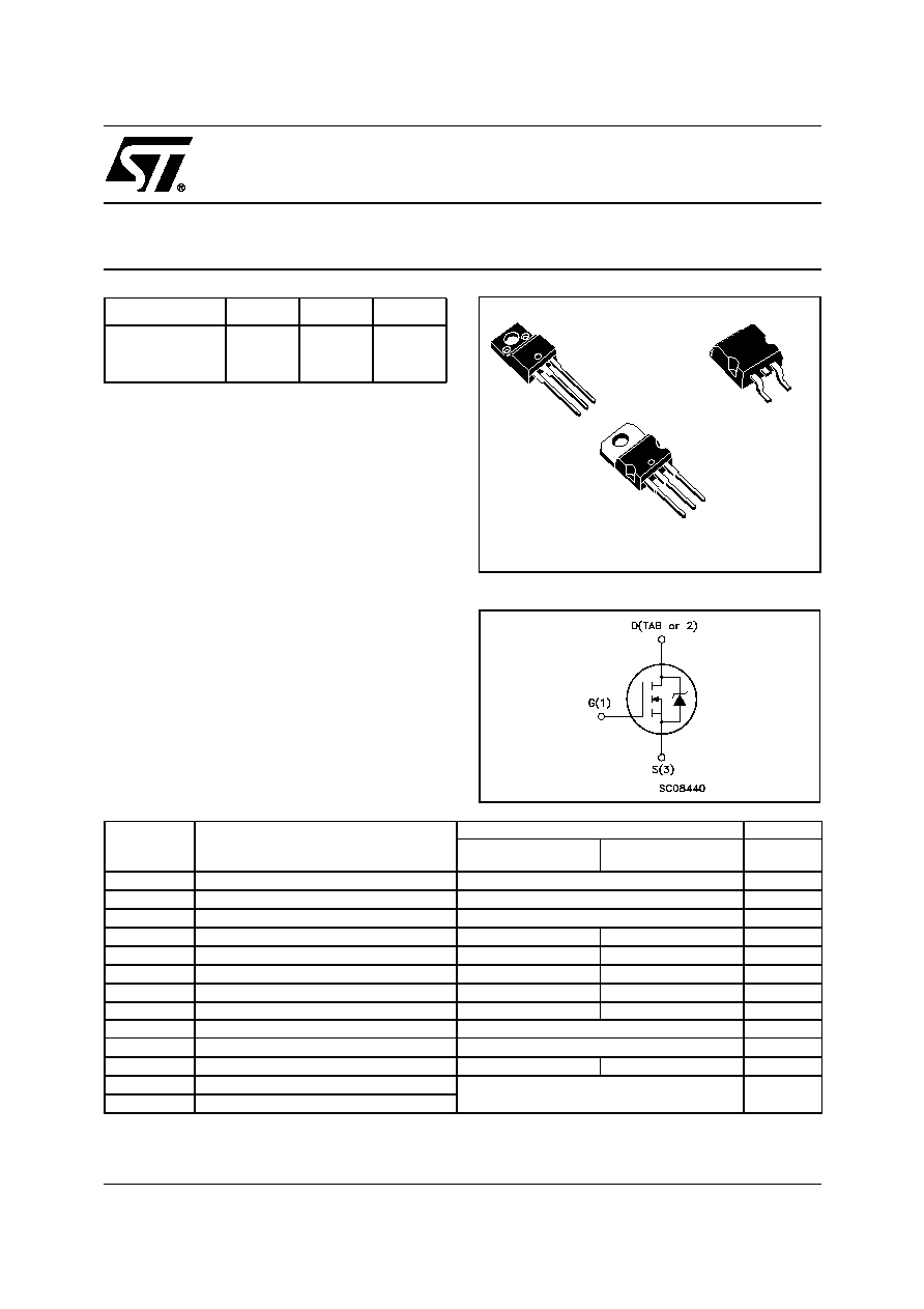
TO-220
1
2
3
TO-220FP
1
3
D
2
PAK
TO-263
(Suffix "T4")
1
2
3
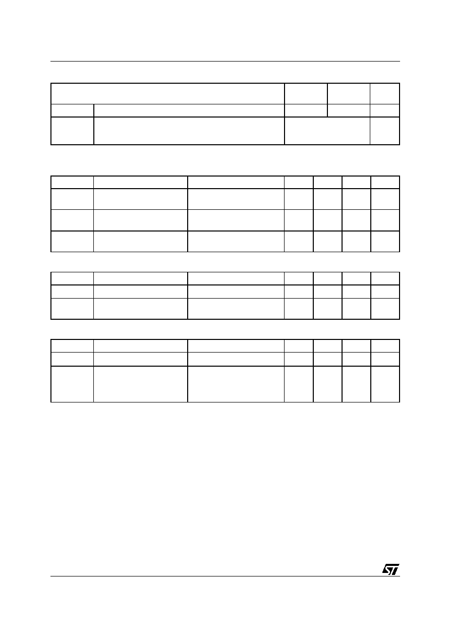
INTERNAL SCHEMATIC DIAGRAM
ABSOLUTE MAXIMUM RATINGS
(
∑)
Pulse width limited by safe operating area.
(*)
Refer to SOA for the max allowable current values on FP-type
due to Rth value
(1) I
SD
80A, di/dt
300A/µs, V
DD
V
(BR)DSS
, T
j
T
JMAX
(2) Starting T
j
= 25
o
C, I
D
= 40A, V
DD
= 37.5V
Symbol
Parameter
Value
Unit
STB75NF75
STP75NF75
STP75NF75FP
V
DS
Drain-source Voltage (V
GS
= 0)
75
V
V
DGR
Drain-gate Voltage (R
GS
= 20 k
)
75
V
V
GS
Gate- source Voltage
± 20
V
I
D
Drain Current (continuous) at T
C
= 25∞C
80
80(*)
A
I
D
Drain Current (continuous) at T
C
= 100∞C
70
70(*)
A
I
DM
(
∑)
Drain Current (pulsed)
320
320(*)
A
P
tot
Total Dissipation at T
C
= 25∞C
300
45
W
Derating Factor
2.0
0.3
W/∞C
dv/dt
(1)
Peak Diode Recovery voltage slope
12
V/ns
E
AS (2)
Single Pulse Avalanche Energy
700
mJ
V
ISO
Insulation Withstand Voltage (DC)
------
2000
V
T
stg
Storage Temperature
-55 to 175
∞C
T
j
Operating Junction Temperature
STB75NF75 STP75NF75 STP75NF75FP
2/11
THERMAL DATA
ELECTRICAL CHARACTERISTICS (T
case
= 25 ∞C unless otherwise specified)
OFF
ON
(*)
DYNAMIC
D
2
PAK
TO-220
TO-220FP
Rthj-case
Thermal Resistance Junction-case
Max
0.5
3.33
∞C/W
Rthj-amb
T
l
Thermal Resistance Junction-ambient
Maximum Lead Temperature For Soldering Purpose
( 1.6 mm from case, for 10 sec.)
Max
62.5
300
∞C/W
∞C
Symbol
Parameter
Test Conditions
Min.
Typ.
Max.
Unit
V
(BR)DSS
Drain-source
Breakdown Voltage
I
D
= 250 µA, V
GS
= 0
75
V
I
DSS
Zero Gate Voltage
Drain Current (V
GS
= 0)
V
DS
= Max Rating
V
DS
= Max Rating T
C
= 125∞C
1
10
µA
µA
I
GSS
Gate-body Leakage
Current (V
DS
= 0)
V
GS
= ± 20 V
±100
nA
Symbol
Parameter
Test Conditions
Min.
Typ.
Max.
Unit
V
GS(th)
Gate Threshold Voltage
V
DS
= V
GS
I
D
= 250 µA
2
3
4
V
R
DS(on)
Static Drain-source On
Resistance
V
GS
= 10 V
I
D
= 40 A
0.0095
0.011
Symbol
Parameter
Test Conditions
Min.
Typ.
Max.
Unit
g
fs (*)
Forward Transconductance
V
DS
= 15 V
I
D
= 40 A
20
S
C
iss
C
oss
C
rss
Input Capacitance
Output Capacitance
Reverse Transfer
Capacitance
V
DS
= 25V, f = 1 MHz, V
GS
= 0
3700
730
240
pF
pF
pF

3/11
STB75NF75 STP75NF75 STP75NF75FP
SWITCHING ON
SWITCHING OFF
SOURCE DRAIN DIODE
(*)
Pulsed: Pulse duration = 300 µs, duty cycle 1.5 %.
(
∑)
Pulse width limited by safe operating area.
Symbol
Parameter
Test Conditions
Min.
Typ.
Max.
Unit
t
d(on)
t
r
Turn-on Delay Time
Rise Time
V
DD
= 37.5 V
I
D
= 45 A
R
G
= 4.7
V
GS
= 10 V
(Resistive Load, Figure 3)
25
25
ns
ns
Q
g
Q
gs
Q
gd
Total Gate Charge
Gate-Source Charge
Gate-Drain Charge
V
DD
= 60 V I
D
= 80 A V
GS
= 10V
117
27
47
160
nC
nC
nC
Symbol
Parameter
Test Conditions
Min.
Typ.
Max.
Unit
t
d(off)
t
f
Turn-off Delay Time
Fall Time
V
DD
= 37.5 V
I
D
= 45 A
R
G
= 4.7
V
GS
= 10 V
(Resistive Load, Figure 3)
66
30
ns
ns
Symbol
Parameter
Test Conditions
Min.
Typ.
Max.
Unit
I
SD
I
SDM
(
∑
)
Source-drain Current
Source-drain Current (pulsed)
80
320
A
A
V
SD
(*)
Forward On Voltage
I
SD
= 80 A
V
GS
= 0
1.5
V
t
rr
Q
rr
I
RRM
Reverse Recovery Time
Reverse Recovery Charge
Reverse Recovery Current
I
SD
= 80 A
di/dt = 100A/µs
V
DD
= 25 V
T
j
= 150∞C
(see test circuit, Figure 5)
132
660
10
ns
nC
A
ELECTRICAL CHARACTERISTICS (continued)
Safe Operating Area for TO-220FP
Safe Operating Area
STB75NF75 STP75NF75 STP75NF75FP
4/11
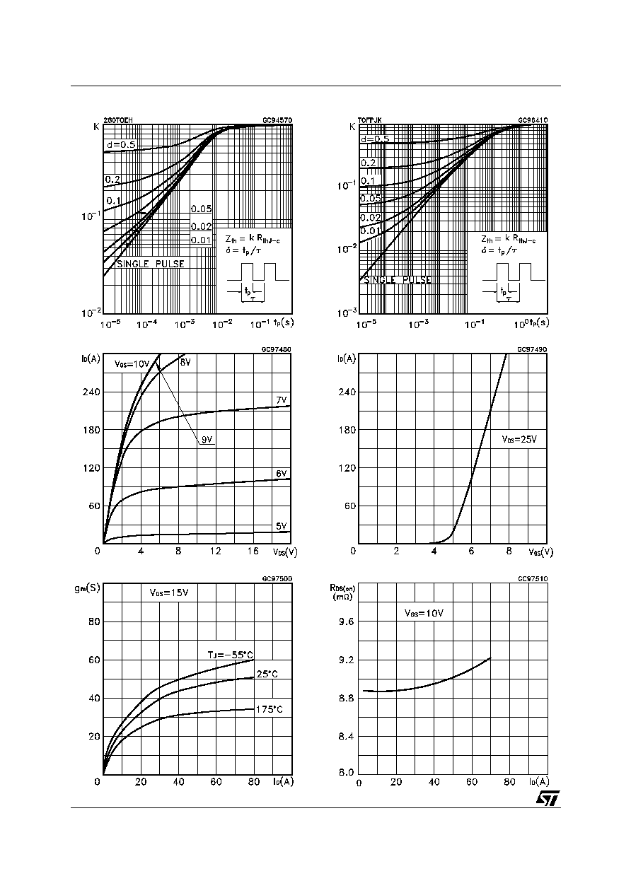
Thermal Impedance
Thermal Impedance for TO-220FP
Output Characteristics
Transfer Characteristics
Transconductance
Static Drain-source On Resistance

5/11
STB75NF75 STP75NF75 STP75NF75FP
Gate Charge vs Gate-source Voltage
Capacitance Variations
Normalized Gate Threshold Voltage vs Temperature
Normalized on Resistance vs Temperature
Source-drain Diode Forward Characteristics
Normalized Breakdown Voltage Temperature